For more than six decades, modern civilization has expanded its intellectual and industrial capabilities on the back of a single physical phenomenon: the movement of electrons through doped silicon channels. But as frontier artificial intelligence models demand gigawatts of power and planetary-scale data centers, the electronic transistor is rapidly running into an immovable physical barrier. It is not Moore’s Law of transistor scaling that is failing first; it is the physics of copper wiring.
At gigahertz frequencies, forcing electrons down nanoscale interconnects generates staggering electrical resistance, capacitive delay, and catastrophic Joule heating. Today, modern AI accelerators dedicate over 60% of their thermal and energy budgets simply to shuttling data between memory banks and compute cores. For decades, computer scientists and physicists have envisioned an ultimate escape hatch: all-optical computing, an architecture where calculations and routing are executed entirely by photons traveling at the speed of light with virtually zero parasitic heat.
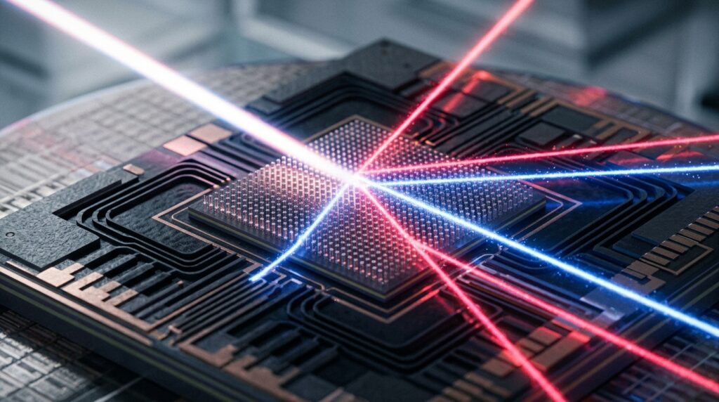
Yet all-optical systems have been perpetually stalled by a fundamental paradox: photons do not easily interact with each other. To steer or switch light, chips have had to rely on cumbersome electronic modulators or slow thermal heaters—reintroducing the very electronic bottlenecks photonics was designed to eliminate. Now, in a landmark investigation published in Nature Nanotechnology, researchers at the California Institute of Technology (Caltech) have shattered that limitation. By engineering an ultrafast nanoscale silicon metasurface, the team has successfully demonstrated the ability to steer and reshape a beam of light using another beam of light in just 74 femtoseconds—74 quadrillionths of a second.
The OEO Penalty: Why Existing Photonics Still Choke on Electricity
To appreciate the magnitude of the Caltech advance, one must examine why current optical interconnects have failed to replace digital electronics wholesale. In today’s hyperscale AI clusters, optical transceivers are widespread, but they operate under a punishing operational tax known as Optical-to-Electrical-to-Optical (OEO) conversion.
Data leaves an electronic tensor core as a burst of voltage, passes into an electro-optic modulator that imprints the bits onto a laser carrier, travels across optical fiber, and hits a photodetector at the destination chip that converts the photons back into electrical charges. Every conversion stage introduces latency, consumes several picojoules per bit, and generates heat. As AI workloads scale from thousands to hundreds of thousands of interconnected chips, these conversion penalties accumulate into an intolerable electronic chokepoint.
True all-optical signal processing requires an optical switch: an optical transistor where one beam of light controls the transmission, deflection, or phase of another beam directly inside the solid state. Historically, attempts to achieve this in silicon faced severe physical compromises:
- Thermo-Optic Modulation: Heating silicon changes its refractive index, but thermal dissipation is glacially slow, capping switching speeds in the kilohertz to megahertz range (microseconds).
- Free-Carrier Dispersion: Injecting electrical charges into silicon alters optical absorption and refraction, reaching gigahertz rates (nanoseconds), but carrier recombination times introduce significant latency and power consumption.
- Mechanical Micro-Mirrors (MEMS): Physically rotating microscopic mirrors allows clean optical routing, but mechanical inertia limits response times to milliseconds.
None of these approaches could match the pure, uninhibited clock frequencies demanded by next-generation computing architectures. What physics required was an instantaneous, non-thermal mechanism operating at the quantum timescale of electrons bound within atoms.
74 Quadrillionths of a Second: Putting the Femtosecond Frontier in Perspective
The Caltech study, spearheaded by lead author Dr. Claudio Hail and senior author Professor Harry Atwater in the Division of Engineering and Applied Science, circumvented electronic carrier dynamics entirely by tapping into the ultrafast optical Kerr effect.
To grasp the staggering velocity of 74 femtoseconds ($74 \times 10^{-15}$ seconds), consider the following physical scales:
- The Speed of Light Horizon: In one second, light travels 300,000 kilometers—nearly reaching the Moon. In 74 femtoseconds, light travels approximately 22 micrometers, roughly a fraction of the diameter of a single human hair.
- Clock Speed Acceleration: The fastest commercial electronic processors operate at clock speeds of approximately 5 GHz (one clock cycle every 200 picoseconds). The Caltech metasurface operates more than 2,700 times faster than a 5 GHz clock cycle, placing optical switching firmly into the multi-terahertz and petahertz (PHz) regime.
- Carrier-Free Physics: Because the switching happens faster than the time it takes for silicon’s crystal lattice to vibrate (phonons) or for free electron-hole pairs to migrate, the system does not heat up or suffer from carrier recombination lag.
“Conventional optical modulation relies on pushing electrons around or heating materials up, which will always be fundamentally sluggish. By designing subwavelength silicon antennas that harness instantaneous nonlinear polarizability, we can use one pulse of light to steer another in tens of femtoseconds. We are manipulating light at the speed of atomic electronic response.”
— Dr. Claudio Hail, Lead Author, California Institute of Technology
The Physics: Amplifying the Optical Kerr Effect with Nanoscale Metasurfaces
How did the Caltech researchers induce light to manipulate light in ordinary silicon, a material typically considered optically linear at moderate powers? The answer lies in nanophotonic metamaterials and structural resonance.
Under intense electromagnetic fields, transparent dielectric materials exhibit the optical Kerr effect: a third-order nonlinear optical phenomenon (governed by the $\chi^{(3)}$ nonlinear susceptibility tensor) wherein the material’s refractive index changes proportionally to the square of the electric field ($n = n_0 + n_2 I$). When the laser pulse passes, the refractive index returns to its baseline virtually instantaneously—within mere attoseconds to femtoseconds.
However, in bulk silicon, the nonlinear Kerr coefficient $n_2$ is minuscule. Under standard conditions, creating a measurable change in refractive index would require laser powers so catastrophic that they would vaporize the chip. The Caltech team resolved this through geometric engineering:
- Subwavelength Silicon Nanopillars: The team fabricated an ultra-thin metasurface comprised of meticulously patterned silicon nanoresonators, each measuring mere tens of nanometers across—smaller than the wavelength of the interacting infrared light.
- Electromagnetic Field Trapping: These nanopillars behave as subwavelength optical cavities supporting Mie resonances. When a control “pump” laser pulse illuminates the surface, the electric field is compressed and trapped within the nanoscale silicon structures, magnifying local optical field intensity by multiple orders of magnitude.
- Transient Phase Gradient Induction: By spatially modulating the intensity profile of the pump pulse across the metasurface array, the team imparted a localized, asymmetric refractive index shift across the silicon interface.
- Dynamic Beam Deflection: When a second “probe” beam of light arrives at the metasurface, it encounters an engineered phase gradient that instantaneously refracts and steers the beam by up to 13 degrees off its original trajectory.
The entire sequence—from the arrival of the control pulse, the field localization, the nonlinear index shift, to the deflection of the probe beam—completes and resets in 74 femtoseconds, leaving no residual thermal footprint on the substrate.
Architectural Matrix: Electronics vs. Classical Photonics vs. Femtosecond Metasurfaces
To understand the structural advantage this discovery delivers to computing architecture, compare the operational parameters across computing generations:
| Architectural Metric | Advanced Electronic CMOS (3nm) | Conventional Silicon Photonics | Caltech Femtosecond Metasurface |
|---|---|---|---|
| Primary Information Carrier | Electrons (Charge flux) | Photons (Guided waves) | Photons (Resonant waves) |
| Switching Mechanism | Electrostatic gate depletion | Thermo-optic / Carrier injection | Enhanced optical Kerr effect |
| Switching Latency | 50 – 200 picoseconds | 1 – 100 nanoseconds | 74 femtoseconds (~1,000x faster) |
| Equivalent Operational Frequency | 3 GHz – 5 GHz | 10 GHz – 50 GHz | 13.5 Terahertz (Theoretical PHz limit) |
| OEO Conversion Required? | N/A (Native electronic) | Yes (Mandatory at logic boundaries) | No (Direct all-optical control) |
| Dominant Physical Bottleneck | RC interconnect delay & Joule heat | Carrier recombination & thermal dissipation | Ultrashort pulse peak power coupling |
Rewiring the AI Supercomputer: Near-Packaged Optics & Optical Neural Networks
The timing of Caltech’s publication coincides with an unprecedented structural crisis in artificial intelligence hardware. Frontier models—now training across clusters of 100,000 or more synchronized accelerators—are bound by what engineers term the “Memory and Interconnect Wall.” Compute chips spend vastly more clock cycles waiting for memory transfers over copper traces than they do performing actual matrix multiplications.
The femtosecond metasurface unlocks three transformative applications for next-generation AI infrastructure:
1. All-Optical Crossbar Routing and Near-Packaged Optics (NPO)
In distributed training topologies, communication latency between accelerator nodes dominates training runtimes. By integrating femtosecond metasurface switches into Near-Packaged Optics (NPO) and Co-Packaged Optics (CPO) architectures, optical routing switches can redirect multi-terabit data streams between memory fabrics and tensor arrays dynamically at femtosecond speeds, completely bypassing electrical packet switches.
2. Photonic Matrix Multiplication at the Speed of Light
Modern transformer neural networks rely heavily on matrix-vector multiplications ($Y = WX$), which constitute over 90% of the mathematical workload in deep learning. In an Optical Neural Network (ONN), these multiplications can be performed passively using diffractive metasurfaces where light waves interfere with one another. Until now, reconfiguring the weights ($W$) dynamically during inference or backpropagation was restricted by slow electro-optic modulators. Femtosecond Kerr metasurfaces provide the theoretical foundation for reconfigurable weights operating at terahertz update frequencies.
3. Extreme-Speed Beam Steering for Free-Space Optical Interconnects
Beyond intra-chip communications, modern hyperscale facilities are exploring free-space optical (FSO) interconnects inside server racks, eliminating heavy fiber cabling bundles entirely. A solid-state device capable of steering optical beams by 13 degrees in under 100 femtoseconds without mechanical gimbals or bulky phased arrays transforms dynamic optical routing in server chasses.
The Engineering Roadmap: From Cleanroom to Foundry
Despite the revolutionary implications, the Caltech research team and semiconductor industry analysts emphasize that several formidable engineering challenges must be surmounted before femtosecond all-optical logic replaces silicon foundries:
- On-Chip Laser Integration: Generating 74-femtosecond control pulses currently requires specialized mode-locked pulsed lasers. Integrating mode-locked femtosecond laser sources directly onto silicon photonics dies alongside continuous-wave (CW) distributed feedback lasers remains an active area of optoelectronic packaging research.
- Energy per Bit Scaling: While the switching process generates zero thermal heating via electron flow, delivering sufficient optical peak power within a 74-femtosecond temporal window demands careful optical cavity engineering to lower switching thresholds into the sub-femtojoule per bit regime.
- CMOS Foundry Compatibility: Because the Caltech metasurface was fabricated using standard silicon rather than exotic, toxic compounds like gallium arsenide or lithium niobate, the design is fundamentally compatible with existing 300mm deep-ultraviolet (DUV) and extreme-ultraviolet (EUV) photolithography lines at commercial foundries such as TSMC and Tower Semiconductor.
“The most encouraging aspect of this breakthrough is the material platform. We didn’t build this from exotic crystals or cryogenic superconductors. This is silicon—the very foundation of modern global industry. That means the path from physical discovery to industrial fabrication is already mapped.”
— Professor Harry Atwater, Senior Author and Howard Hughes Professor of Applied Physics and Materials Science, Caltech
Key Takeaways for Technology Leaders
- 74-Femtosecond All-Optical Switching: Caltech researchers have demonstrated direct optical beam steering and reshaping using a silicon metasurface in 74 femtoseconds—thousands of times faster than electronic clock limits.
- Eliminating the OEO Chokepoint: Light controls light directly via an amplified optical Kerr effect, bypassing the latency, thermal dissipation, and power consumption of optical-to-electrical conversions.
- Subwavelength Nanoscale Physics: Subwavelength silicon nanopillars amplify nonlinear third-order optical susceptibility without triggering free-carrier dispersion or crystal lattice heating.
- AI Supercomputing Acceleration: Unlocks all-optical crossbar switches, ultra-low-latency Co-Packaged Optics (CPO), and reconfigurable Optical Neural Networks capable of processing machine learning tensors at light speed.
- Standard Silicon Substrate: Built using foundry-compatible silicon, establishing a viable commercial roadmap toward industrial silicon photonics integration.